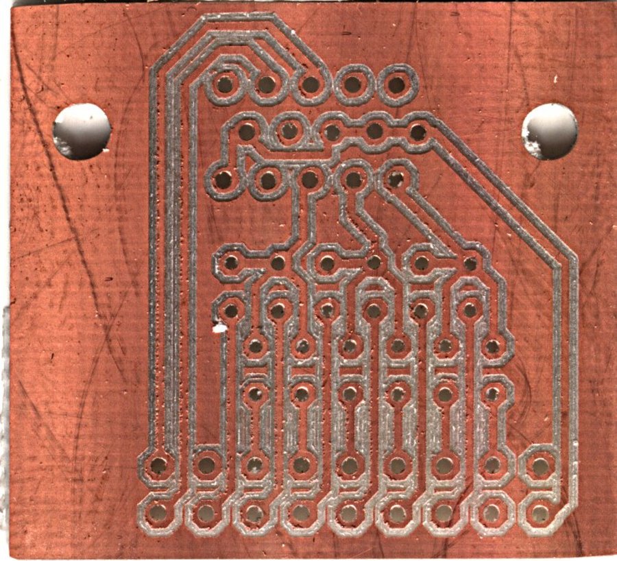
This board took about 10 minutes of milling and tool changing time, plus another 5 minutes for setup and touching off. Compared to earlier boards I've shown, the main change is to use a 1/32" precisebits diamond-cut router bit instead of the 1/16" 2-flute mill I usually use for milling large holes and cutting out the board from the larger copper-clad blank. This bit turns the board substrate into fine dust, a few clumps of which can be seen in the board scan. I ran it at a very conservative 4IPM this time around, but I think I could run it faster.
If you look at the full-size circuit board scan, you'll notice three main problems: the "circular" pads of the HD15 connector are pretty irregular; the octagonal pads are lopsided; and drills are often off-center in their pad. I attribute all these things to backlash. Besides re-measuring and entering the values for backlash on X and Y, I don't think there's anything easy to do about this. Anyway, the results are tolerable.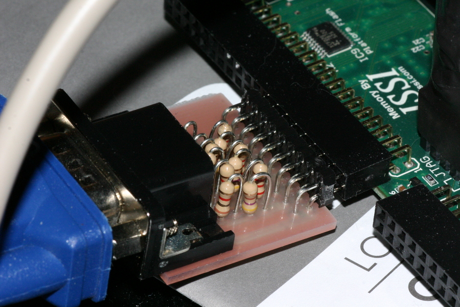
(another problem is the small uncleared areas of copper are more of a trade-off than a problem: I could do more passes, or do a pass with an end-mill, at the expense of increased milling time)
Its purpose is to turn 14 GPIOs on the A2 connector of the S3BOARD FPGA into a 12-bit (4096-color) VGA interface. Projects I might make with this would be a retro-style gaming system, emulation of classic home systems or classic arcade systems. Or maybe I'll work on turning the FPGA-based logic analyzer into a device that doesn't need a PC to operate--just a mouse and a VGA monitor.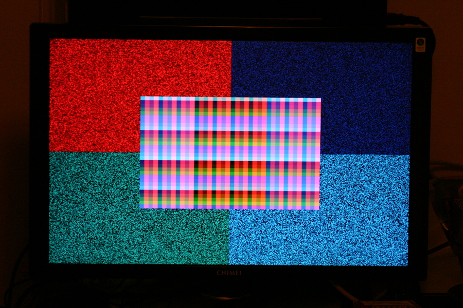
(Or maybe I'll just display that test pattern and then let this board find
its way to the back of the junk bin)
(originally posted on the AXIS blog)
Entry first conceived on 26 August 2008, 1:46 UTC, last modified on 15 January 2012, 3:46 UTC
Website Copyright © 2004-2024 Jeff Epler